¶ Missing Components
A few components were not loaded during assembly at Screaming Circuits.
¶ Card Edge Connector
The card edge connector should be loaded on the bottom of the active board PCB. Care should be taken when inserting the part to not bend the pins. Also make sure that it lies flat with the PCB.
¶ MicroZed Connectors
The JX1/JX2 should be loaded with the MicroZed connectors.
Some tips for soldering them:
- Solder a few feet with a MicroZed connected to the connector and being pressed on. This will ensure that the connectors are aligned well and lie flat.
- Easiest way to apply the solder is to lie a length of thin solder wire along the feet and jab it with a solder iron. This might create a few shorts on adjacent feet. However the solder wick does a good job at removing the extra solder .
- Check that all feet are soldered. A good wayt to check this is to run a pair of tweezers on the feet while observing them under a microscope. None should move.
¶ 2x MCP3428
The MCP3428 should be soldered to positions U206, U207 and U208.
There is already solder on the pads from the commerial SMD loading. Only only has to place the package on the pads and press the feet with solder iron.
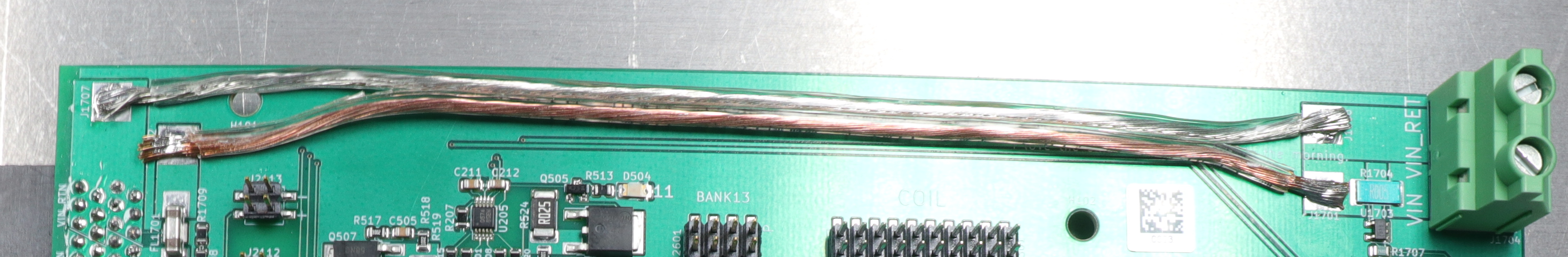
¶ Vin Wire
Solder a wire between the Vin pads. The length of the wire is 17 cm for VIN. For VINrtn it is a bit shorter, as can be see in the picture below. Make sure to leave space for the mounting hole.
¶ Errata
¶ -5V Current Measurement
The differential amplifier on the negative power rail of the active board seems to have trouble with negative common mode voltages. It causes an increase in current.
Fix: Remove U1704.
¶ CMD Multiplexers
The pinout of the multiplers used for the CMD lines is wrong. Currently, the CMD_IN and CMD_OUT for a given Powerboard are on the same mux channel. Thus they cannot be enabled at the same time.
Fix: Use the direct connection instead of the multiplexers.
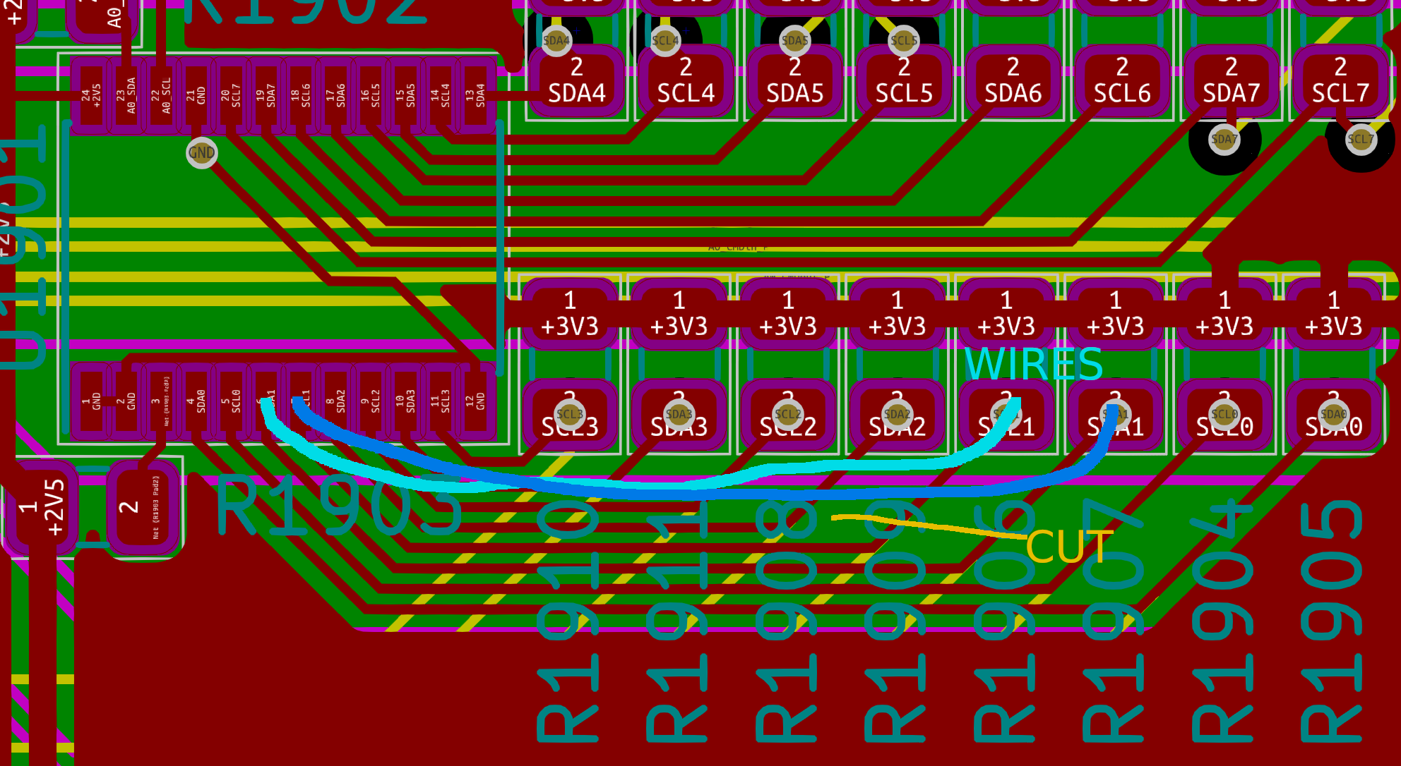
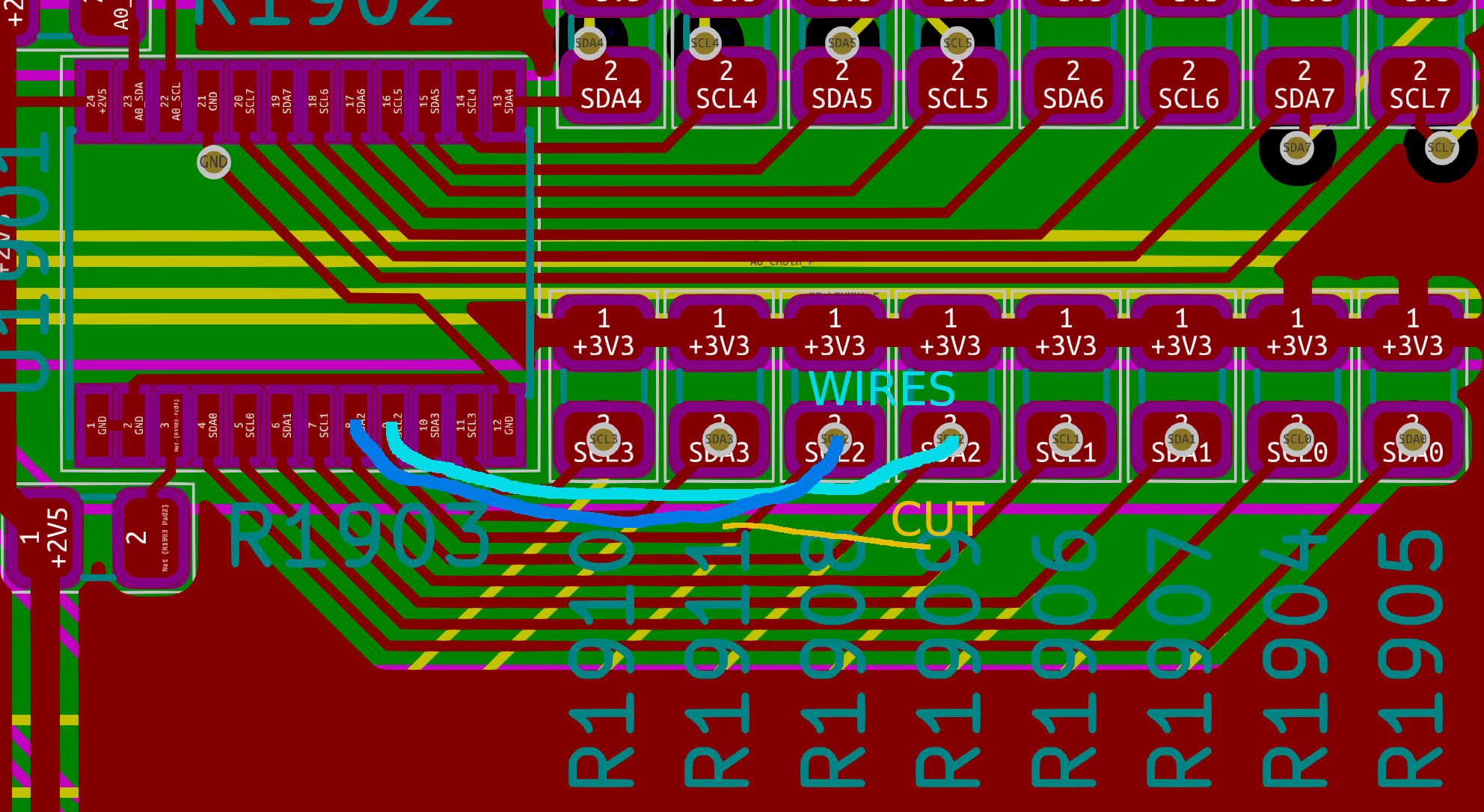
¶ I2C SCL/SDA Lines Swapped
Several of the I2C channels have the data and clock lines swapped.
Fix: Manually cut and swap traces using blue wires. The final result should look as follows. A more detail description of which traces to fix follows.
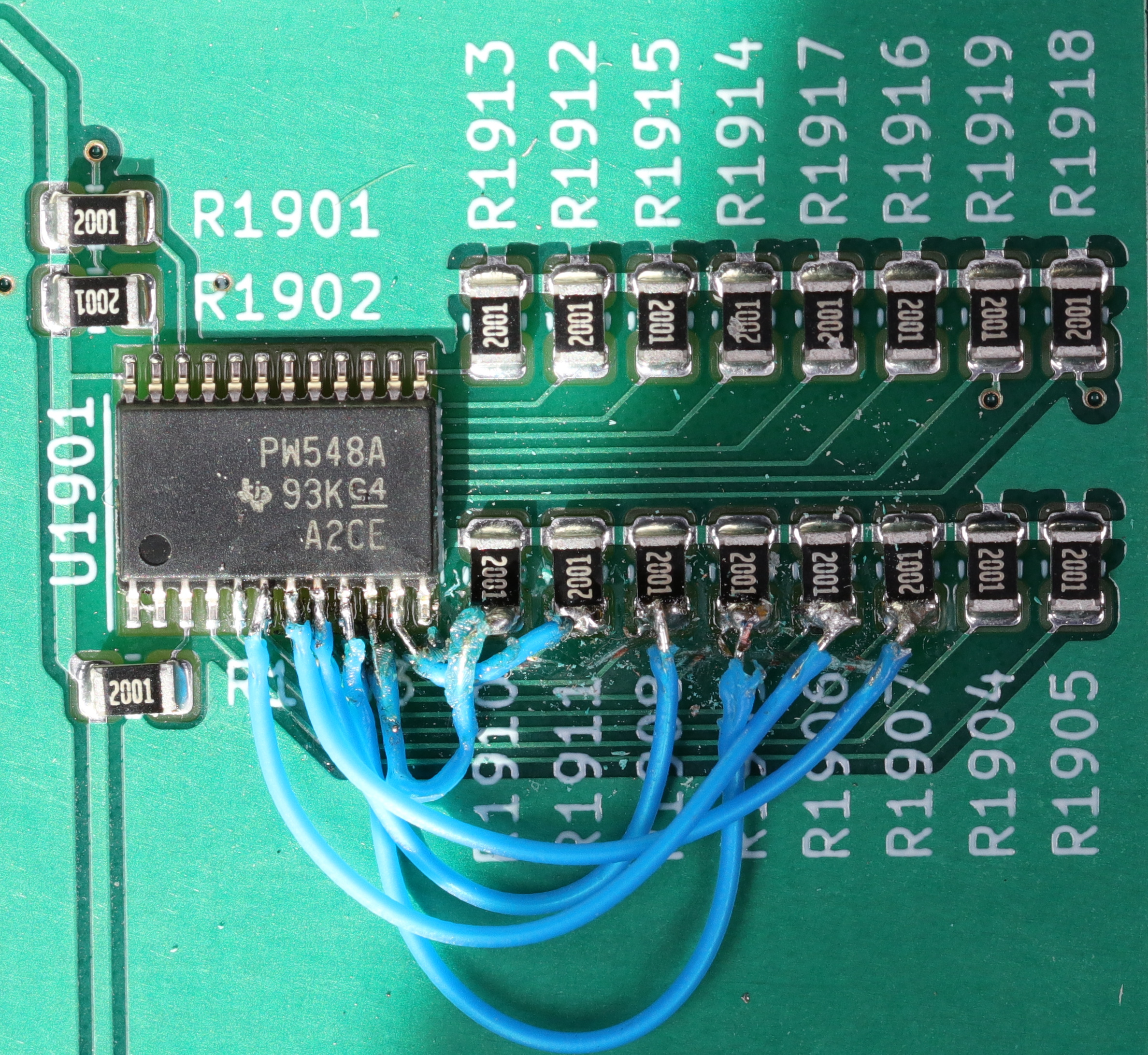
¶ I2C1 Blue Wires
¶ I2C2 Blue Wires
¶ I2C3 Blue Wires

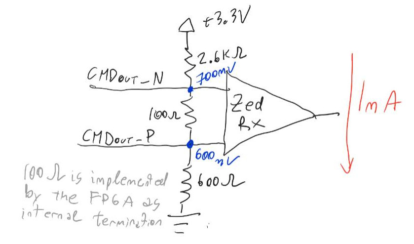
¶ Fail-safe Active Bias for CMDout
The AMACv2 differential CMDout driver is disabled when not sending data. This is an unstable state for the LVDS receiver in the MicroZed. The result is a noisy interpratation of digital 0 and 1. The following fail-safe bias using a small nominal current needs to be added to each circuit. The 100Ω is the internal termination of the FPGA. The 2.6kΩ and 600Ω resistors are rough values that result in a ~650 mV common mode. In the following example, resistor values of 2.61kΩ and 600Ω were used.
¶ Applying the Fix
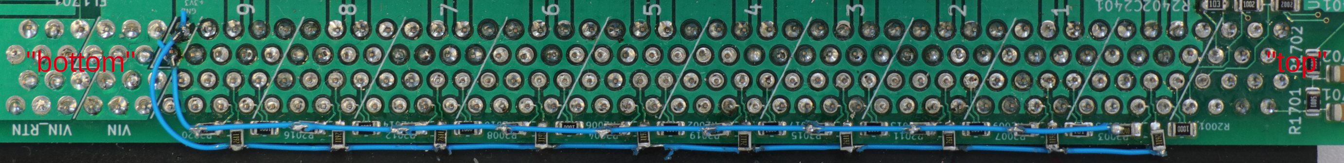
The following are detailed pictures of the fix. The steps to reproduce it are outlined next.

The implementation can be done with the following steps.
- The 2.6kΩ and 600Ω resistors need to be added to the unused pads meant for the unloaded external termination of CMDout (R2020, R2016, R2012, R2008, R2004, R2019, R2015, R2011, R2007 and R2003). See picture above for the orientation of how they should be attached.
- The 2.6kΩ resistor should be loaded on the top (towards HVin) pad and stick out towards the edge card connector
- The 600Ω resistor should be loaded on the bottom (towards LVin) pad and point towards it
- Cut two long (~30 cm) pieces of wire that will be used to connect the other ends of the resistors to +3.3V and GND.
- Solder one end of the wire to the bottom of the 2.6kΩ CMDout0 resistor.
- Align the same wire to the bottom of the 2.6kΩ CMDout1 and solder it. Use the solder iron to melt the insulation in the correct spot without cutting the wire. Clean the resistor tip often as the plastic will gunk it up.
- Repeat step 4 for all positions.
- Solder the second wire to the top of the 600Ω CMDout0 resistor.
- Align the same wire to the top of the 600kΩ CMDout1 resistor and solder it. As before, use the solder iron to melt the insulation in the correct spot without cutting the wire. Clean the resistor tip often as the plastic will gunk it up.
- Repeat step 7 for all positions.
- Solder the dangling end of the first wire (2.6kΩ) to the +3.3V pin on the edge card connector PCB pin.
- Solder the dangling end of the second wire (600Ω) to the GND pin on the edge card connector PCB pin.
- Make sure to test the patch before plugging in a carrier card. The instructions are in the next section.
¶ Testing the Fix
The following instructions are to test that the batch has been implemented correctly. Do the test before plugging in a carrier card.
- Connect a MicroZed to the active board and all the necessary cables (ethernet and +5V/-5V).
- Power the active board using +5V/-5V.
- Use a multimeter to measure the voltage between ground and the PCB side of each resistor. The values should be roughly 700 mV and 600 mV for the 2.6kΩ and 600kΩ resistor ends. See diagram for clarification of the ends points to measure.
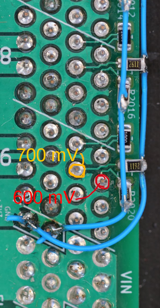
- Repeat this for all channels. If any values are wrong, check for short or bad solder between the resistor and wire.
Side Note: Resistors could possibly short from solder underneath
¶ Saturating HV sense
The 5kΩ resistors used to sense the HV current saturate at 1mA. They should be replaced with 3.24kΩ resistors instead.
This corresponds to references R701, R801, R901, R1001, R1101, R1201, R1301, R1401, R1501, R1601.
¶ Updating Range of Variable Loads
A 100mΩ resistor should be used instead of 25mΩ to set the load current to reduce the sensitivity to mV level noise. The DAC voltage divider then needs to be updated to maintain the 0-4 Amp range.
Replace all 2512 sized resistors (R307, R314, R319, R324, R407, R414, R419, R424, R507, R514, R519 and R524) with 100mΩ.
Replace lower half of the DAC voltage divider (R309, R316, R321, R324, R402, R409, R416, R421, R502, R509, R516 and R521) with 16.9kΩ.
¶ Pull-Down Output Readout
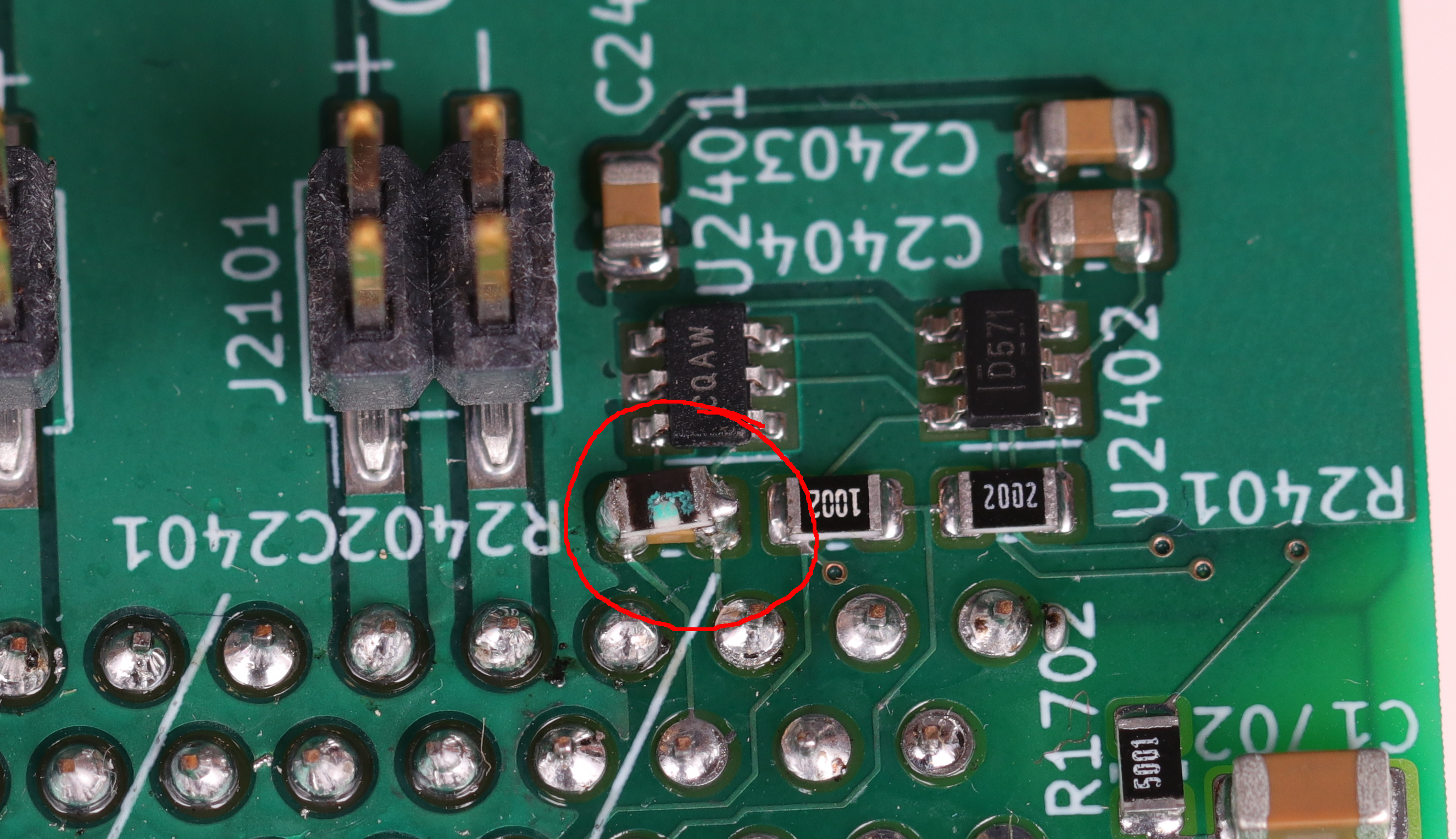
The active board uses a differential ADC to readout the different outputs (ie: bPOL output, LDen output) of the Powerboard. If a wirebond is missing, then the input to the ADC is left floating and the measurement is non-physical. A pull-down resistor should be placed on the ADC input. This results in a 0V input with a wirebond missing. This resistor needs to have a large value (~10 MΩ) as some AMAC outputs have a 10kΩ resistor in series.
Fix: Place a 5-10MΩ resistor on top of the C2401 capacitor.