¶ Table of Contents
- Quad Hybrid Design
- Data Adapter Card
- Data Pigtail
- Power Adapter Card
- Power Pigtail
- Setup
- List of Digital Quads
- Connectivity Example
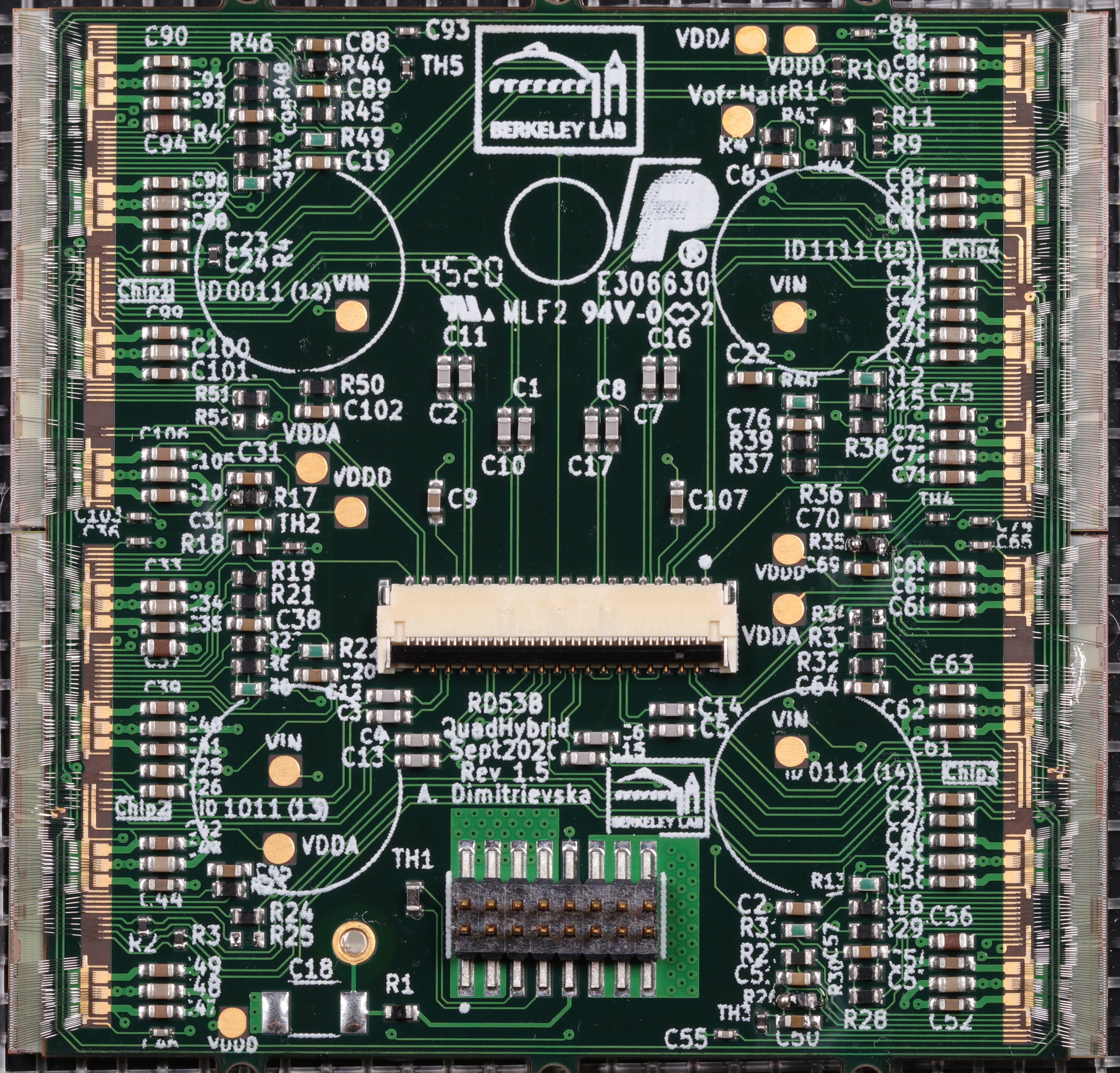
¶ Quad Hybrid Design
The design files for the quad hybrid is here:
https://gitlab.cern.ch/adimitri-group/kicad/rd53b_quad_hybrid/-/tree/lbl_layout_Rev1.5
The higher 2-bits for the ChipID are routed through the connector. The lower 2-bits are hard coded with wirebonding. The chipIDs on the module by default is (it is also labeled on the hybrid):
| #Chip | ChipID |
|---|---|
| Chip 1 | 12 |
| Chip 2 | 13 |
| Chip 3 | 14 |
| Chip 4 | 15 |
BoM changes:
- R_Vref_adc (R44, R35, R26, R17) 84.5 Ohm -> 84.5 kOhm
- RextA (R47, R38, R29, R20) 698 Ohm -> 1000 Ohm
- RextD (R51, R42, R33, R24) 825 Ohm -> 866 Ohm
- RoffsetLP (R49, R40, R31, R22) 10 kOhm -> 8.76 kOhm
Data routing:
| #Chip | Data Line | Destination |
|---|---|---|
| Chip 1 | GTX0 | DATA_IN3_Chip4 |
| Chip 1 | GTX1 | DATA_IN2_Chip4 |
| Chip 1 | GTX2 | Connector |
| Chip 1 | GTX3 | Connector |
| Chip 2 | GTX0 | Connector |
| Chip 2 | GTX1 | Connector |
| Chip 2 | GTX2 | DATA_IN1_Chip4 |
| Chip 2 | GTX3 | Not Connected |
| Chip 3 | GTX0 | DATA_IN1_Chip2 |
| Chip 3 | GTX1 | DATA_IN0_Chip2 |
| Chip 3 | GTX2 | DATA_IN0_Chip4 |
| Chip 3 | GTX3 | Connector |
| Chip 4 | GTX0 | Connector |
| Chip 4 | GTX1 | Connector |
| Chip 4 | GTX2 | Not Connected |
| Chip 4 | GTX3 | Not Connected |
Summary of v1.5 quad hybrids:
| #Hybrid | Comment | Destination |
|---|---|---|
| 01 | for resistivity measurements | irradiation |
| 02 | LDO, high current | Quad02 |
| 03 | LDO, working | Quad03 |
| 04 | LDO, working | Quad04 |
| 05 | SLDO, working | Quad05 |
| 06 | LDO, working | Quad06 |
| 07 | LDO, working | Quad07 |
| 08 | SLDO, working | Quad08 |
| 09 | shipped to CERN | CERN |
| 10 | shipped to CERN | CERN |
| 11 | SLDO, ITkPixV1.0 | Quad11 |
| 12 | SLDO, ITkPixV1.1 | Quad12 |
| 13 | SLDO, ITkPixV1.1 | Quad13 |
| 14 | SLDO, ITkPixV1.1 | Quad14 |
| 15 | SLDO, ITkPixV1.1 | Quad15 |
| 16 | SLDO, ITkPixV1.1 | Quad16 |
| 17 | SLDO, ITkPixV1.1 | Quad17 |
| 18 | SLDO, ITkPixV1.1 | Quad18 |
| 19 | SLDO, ITkPixV1.1 | Quad19 |
| 20 | Shipped to Japan | Japan |
| 21 | Shipped to Japan | Japan |
| 22 | SLDO, ITkPixV1.0 Module | QuadR01 |
| 23 | SLDO, ITkPixV1.1 | Quad23 |
| 24 | Eric, scan | CPPM |
| 25 | pull tests | irradiation |
¶ Wirebonding diagrams
- Chip 1 rd53b_hybrid_wirebonds_chip1.pdf
- Chip 2 rd53b_hybrid_wirebonds_chip2.pdf
- Chip 3 rd53b_hybrid_wirebonds_chip3.pdf
- Chip 4 rd53b_hybrid_wirebonds_chip4.pdf
¶ Iref trimming
There are multiple ways to trim Iref on RD53B chips (the details are given in the note https://twiki.cern.ch/twiki/pub/RD53/RD53BTesting/AP_Note_Iref_Trimming_v0_2.pdf). The Iref on the module has to be trimmed according to Voffset. There are 4 trim bits on RD53B chip and they are wirebonded to the GND by default (0000), corresponding to chip pads 47, 48, 49 and 50. The Iref trim bits internaly in the chip are pulled-up to Vdd_PRE.
The Iref trim bonds should be pulled according to wafer probing data which is available in production DB (example for one chip https://uuapp.plus4u.net/ucl-itkpd-maing01/dcb3f6d1f130482581ba1e7bbe34413c/testRunView?id=62278e2480e95c000a5c80e7). The Iref trim bit in this example is 7, which is 1110 that corresponds that first 3 trim bits are high and the forth one is pulled to the GND. Therefore, only pad 50 should have a wirebond to GND, and the wirebonds from pads 47, 48 and 49 should be pulled out.
Procedure for Iref trimming when there is no available wafer probing data:
Measure the voltage drop across the R_Voffset, which is 24.9 kOhm (0.1 % presicion), labeled R5, R6, R16 and R15 for Chips 1 to 4 respectivly. The reference current through Voffset resistor is multiplied 5 times (Figure 15 in RD53B manual), from nominal 4 uA. The general trend measured on ITkPixV1.0 chips is that the Iref changes by 0.055 uA per trim bit. So, after measuring the voltage drop across the R_Voffset resistor, the difference wrt to 4 uA has to be divided by 0.055 uA to get the ideal trim bit value.
Example:
- All Iref trim bits are set to 0 (0000)
- Measure voltage drip across R_Voffset resistor: 437.17 mV which gives current of 17.477 uA
- after dividing the measured current through the Voffset resistor the Iref is 3.495 uA
- the difference compared to ideal Iref is: 4 uA - 3.495 uA = 0.505 uA
- if we use 0.055 uA per trim bit: 0.505 uA / 0.055 uA = 9.17
- ideal trim bit should be 9 (1001)
- which means that the first and last iref trim bit wirebond has to be pulled out from the module
¶ Data Adapter Card
There are 3 different versions of the data adapter cards:
- 4 DisplayPort Version where each chip is routed to its own DisplayPort: https://gitlab.cern.ch/adimitri-group/kicad/rd53b_quad_data_adaptercard
- 1 DisplayPort Version where one data line from each chips is routed on a single DisplayPort: https://gitlab.cern.ch/adimitri-group/kicad/rd53b_quad_data_adaptercard/-/tree/1DP_adapter
- 1 DisplayPort Version with CMD Forwarding where one data line from each chips is routed on a single DisplayPort and the CMD is provided from another DisplayPort: https://gitlab.cern.ch/adimitri-group/kicad/rd53b_quad_data_adaptercard/-/tree/1DP_CMDFwd_adapter
Each of the DisplayPort GNDs is isolated from a module GND with a capacitor, since the AC coupling between module and DAQ GND is done on the module, the capacitors on the Data Adapter Cards should be loaded with jummpers (0 Ohm resistor, 0402 imperial size). There is a pin header for LPEnable. There is also a pinheader for 2 highest bits of the ChipID. For CMD forwarding one should connect the ChipID to GND in order to change addresses of the chips in the module to which CMD has been forwarded. There is a pinheader to read the VMUX registers of each chip. Since data lines are double AC coupled (on the module and DAQ side), 10k resistors to GND have been added to all the data lines.
Summary table about produced data adapter cards:
| Power Adapter Cart | Location | Comment |
|---|---|---|
| 4DP 01 | setup @washbear | populated |
| 4DP 02 | setup @Danny | not-populated |
| 4DP 03-09 | not used | not-populated |
| 4DP 10 | shipped to CERN | not-populated |
| 1DP 01 | setup @washbear | populated |
| 1DP 02 | setup @inkfish | populated |
| 1DP 03-10 | not used | not-populated |
| 1DPCMDF 01 | setup @washbear | populated |
| 1DPCMDF 02-10 | not used | not-populated |
¶ Data Pigtail
The design files of the data pigtails is here:
https://gitlab.cern.ch/adimitri-group/kicad/rd53b_datapigtail_39pos/-/tree/Rev1.1a
There are total 54 pigtails produced with 100 Ohm controlled differential impedance, 10 cm long. All are labeled from 01-54.Summary table:
| Data Pigtail | Location |
|---|---|
| 01 | Quad01 |
| 02 | not used, white box |
| 03 | Quad03 |
| 04 | Quad04 |
| 05 | Quad05 |
| 06 | Quad06 |
| 07 | Quad07 |
| 08 | Quad08 |
| 09 | shipped to CERN |
| 10 | shipped to CERN |
| 11 - 53 | white box |
| 54 | shipped to CPPM |
¶ Power Adapter Card
The design files of the power adapter cards are here:
https://gitlab.cern.ch/adimitri-group/kicad/rd53b_quad_power_adaptercard
The card supports two connectors for LV:
- molex connector (same as on SCC)
- spring terminal block (same as on the RD53A quad power adapter cards)
There are pinheaders for LP Enable signal as well as pinheaders and location for voltage divider for the NTC. The HV connector is the LEMO (same as the one on SCC). The interface to the module is through a FTM connector (same as on the module).
There are total 10 power adapter cards produced (order of 10 more will be placed). There is FR4 stiffner on each of the side of the pigtail and the copper thicnkes is 47 um per layer. The total measured resistance of the pigtail is about 30 mOhm (taking into account the contact resistance of the FTM connectors too).
The cards are labeled from 01 to 10. This is a short summary table.
| Power Adapter Cart | Location | Comment |
|---|---|---|
| 01 | setup @washbear | populated |
| 02 | setup @washbear | populated |
| 03 | setup @inkfish | populated |
| 04-09 | not used | not-populated |
| 10 | shipped to CERN | not-populated |
¶ Power Pigtail
There are total 52 power pigtails produced, 10 cm long. All are labeled from 01 - 52. The design files are here:
https://gitlab.cern.ch/adimitri-group/kicad/rd53b_powerpigtail_16pos/-/tree/Rev1.1a
It needs 2 CLM connectors to be populated on each side. Only first 10 have been populated until now. They are produced in panels, 4 pigtails per pannel. Summary table:
| Power Pigtail | Location | Comment |
|---|---|---|
| 01 | Quad01 | populated |
| 02 | not used, white box | populated |
| 03 | Quad03 | populated |
| 04 | Quad04 | populated |
| 05 | Quad05 | populated |
| 06 | Quad06 | populated |
| 07 | Quad07 | populated |
| 08 | Quad08 | populated |
| 09 | shipped to CERN | populated |
| 10 | shipped to CERN | populated |
| 11 - 52 | white box | not populated |
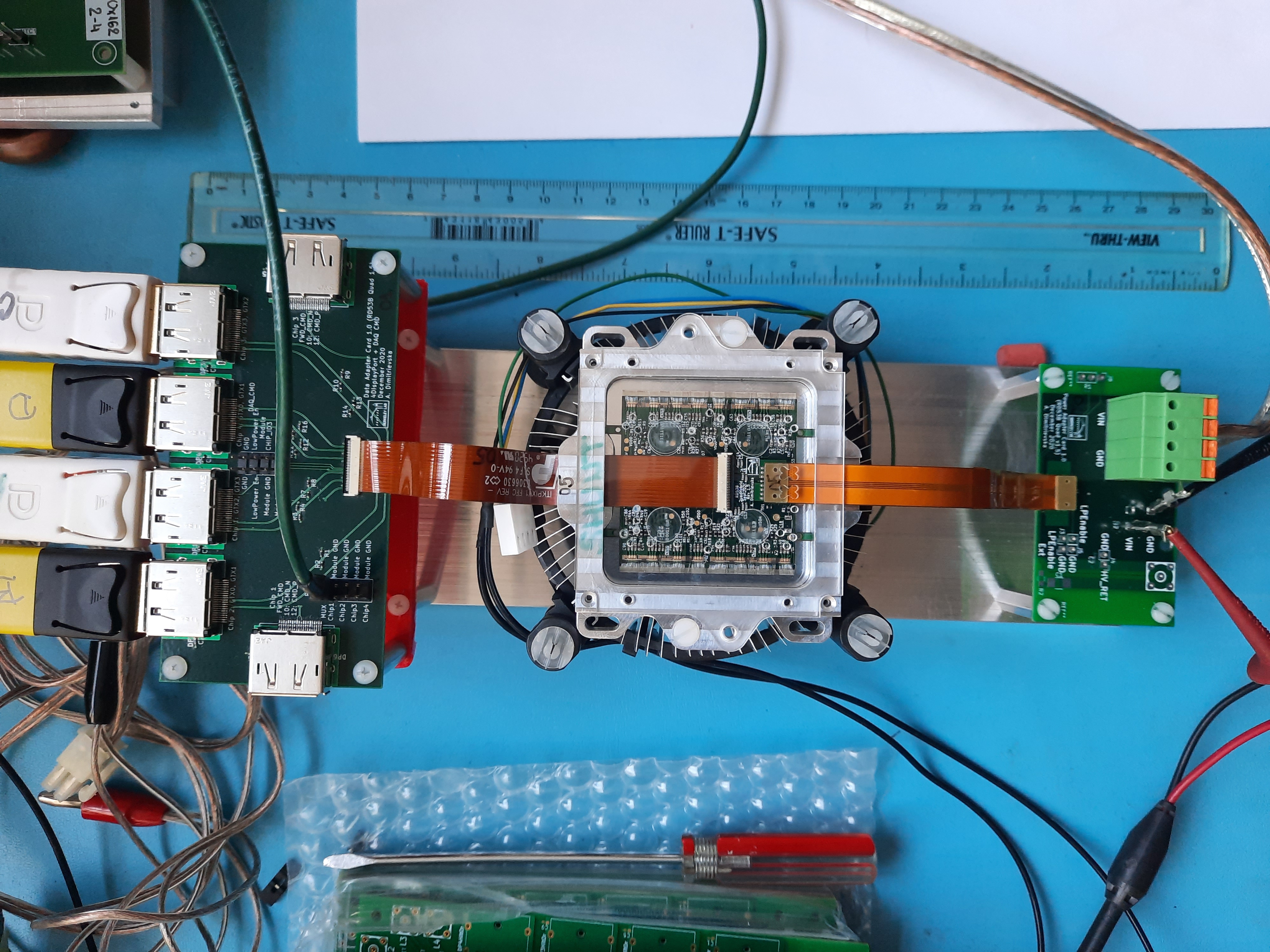
¶ Setup
There are 30 quad carriers which are adapted for ITkPixv1/v1.1 quads. Since they are not labeled, I am adding a number on the top part after each carrier is assembled. There are 8 carriers assembled until now: 01 - 08
The power and data pigails are attached to one quad when placed into carrier. Summary table of all parts used in a setup:
| Carrier | Quad Hybrid | Data Adapter Card | Data Pigtail | Power Adapter Card | Power Pigtail | Comment |
|---|---|---|---|---|---|---|
| 01 | 01 | - | 01 | - | 01 | only flex, Vin and GND wirebonded, used for flex resistance measurements |
| 02 | - | - | - | - | - | empty |
| 03 | 03 | - | 03 | - | 03 | SLDO mode, Voffset Iref trim |
| 04 | 04 | - | 04 | - | 04 | LDO mode, Voffset Iref trim |
| 05 | 05 | - | 05 | - | 05 | SLDO mode, Voffset Iref trim |
| 06 | 06 | - | 06 | - | 06 | LDO mode, Voffset Iref trim |
| 07 | 07 | - | 07 | - | 07 | LDO mode, Voffset Iref trim |
| 08 | 08 | - | 08 | - | 08 | SLDO mode, Voffset Iref trim |
| 09 | ||||||
| 10 | ||||||
| 11 | 11 | - | 11 | - | 11 | |
| 12 | 12 | - | 12 | - | 12 | |
| 13 | 13 | - | 13 | - | 13 | |
| 14 | 14 | - | 14 | - | 14 | |
| 15 | 15 | - | 15 | - | 15 |
¶ Single Quad Setup
There are plastic plates with 4 mounting holes on each end for power and 1DP data adapter card which can be used as a single quad test setup. Each quad is colled with PC fan. The example picture is:
Since the mounting holes are for the 1DP version of the data adapter card, there is a 3D printed plate which enables mounting of the 4DP data adapter card on top. The design is done in Fusion3D and printed on Raise3D printer, the design is shared here:
To 3D print it one needs to install IdeaMaker from Raise3D page and convert the stl file to gcode with template for the filament which will be used for printing. Details are pinned on the Strixel mattermost channel (which used to be 3D printing channel only):
https://mattermost.web.cern.ch/berkeleylab/channels/3dprinter-pixellab
¶ SP Chain Setup
The 8 black plastic holders are designed for the SP chain setup with 4 mointhing holes on each end for power and 1DP data adapter card.
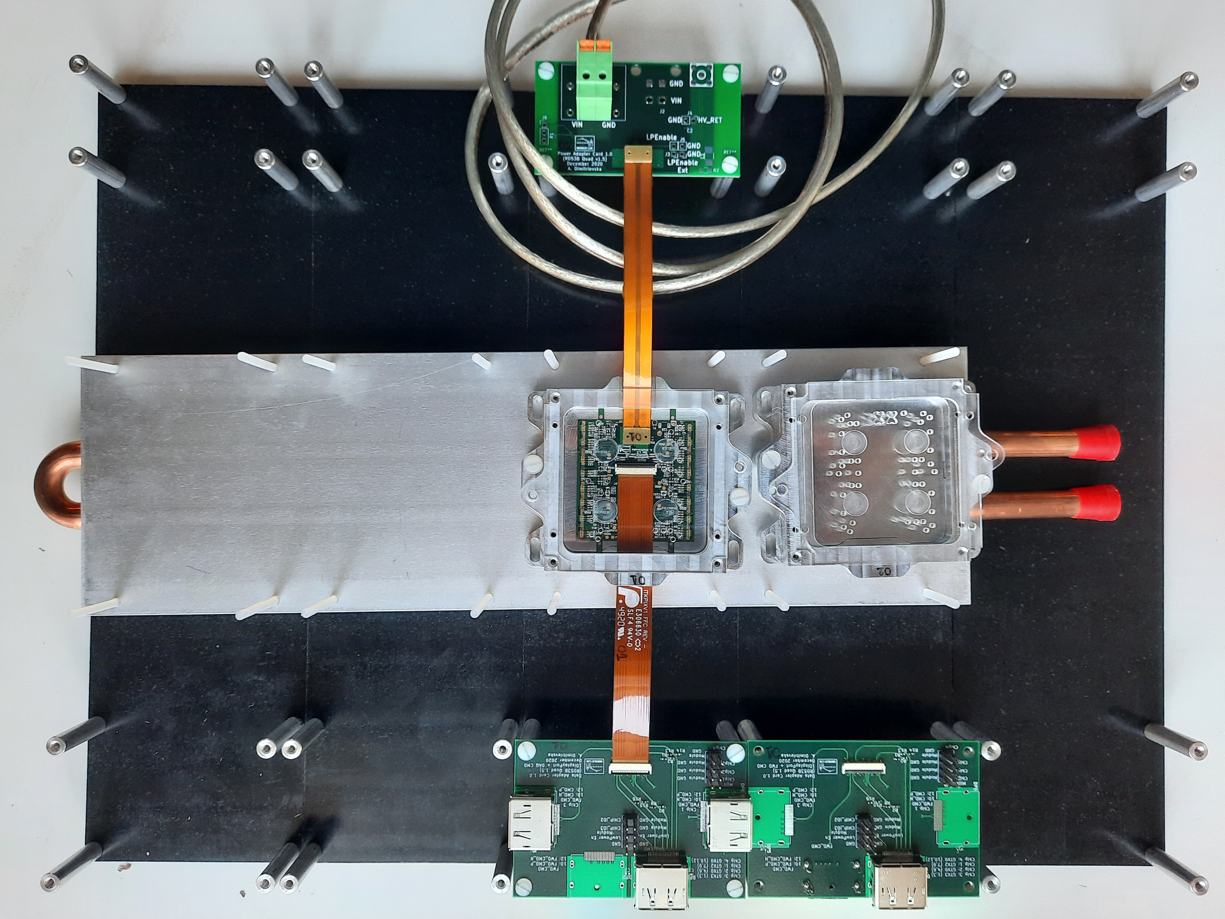
The Al cooling plate has holes so that the quad carriers can be fixed with a aluminum peace on top - which would pervent from opening the top covers. It would be better if there are holes so that the carrers are dirrectly attached. In principle there are 4 slots on each carrier which can be used to mount the carriers to the cooling plate.
¶ List of Digital Quads
LBL PCB v1.5
| Hybrid | Carrier | Chip1 Id | Chip2 Id | Chip3 Id | Chip4 Id | Configuration | Comment | Location |
|---|---|---|---|---|---|---|---|---|
| 02 | - | 0x10A98 | 0x10A88 | 0x10A89 | 0x10A99 | LDO | ITkPixV1.0, too high current 14A, initial wirebonding wrong | Oklahoma |
| 03 | 03 | 0x10AB8 | 0x10AA8 | 0x10AA9 | 0x10AB9 | SLDO | ITkPixV1.0, Iref trim - Voffset | CERN |
| 04 | 04 | 0x10ABA | 0x10AAA | 0x10AAB | 0x10ABB | LDO | ITkPixV1.0, Iref trim - Voffset | Japan |
| 05 | 05 | 0x10A9A | 0x10A8A | 0x10A8B | 0x10A9B | SLDO | ITkPixV1.0, Iref trim - Voffset | Argonne |
| 06 | 06 | 0x10AD8 | 0x10AC8 | 0x10AC9 | 0x10AD9 | SLDO | ITkPixV1.0, Iref trim - Voffset | Oklahoma |
| 07 | 07 | 0x10ACA | 0x10AAC | 0x10AAD | 0x10ACB | LDO | ITkPixV1.0, Iref trim - Voffset | 6007 |
| 08 | 08 | 0x10A9C | 0x10A8C | 0x10A8D | 0x10A9D | SLDO | ITkPixV1.0, Iref trim - Voffset | 6007-Taisei -> CERN(Paris) |
| 09 | CERN | |||||||
| 10 | CERN | |||||||
| 11 | 11 | 0x10A18 | 0x10A28 | 0x10A38 | 0x10A48 | SLDO | ITkPixV1.0 | 6007 |
| 12 | 12 | 0x16285 | 0x162A5 | 0x162C5 | 0x162C7 | SLDO | ITkPixV1.1 | SP Chain, 6007 |
| 13 | 13 | 0x16236 | 0x16256 | 0x16266 | 0x16292 | SLDO | ITkPixV1.1 | SP Chain, 6007 |
| 14 | 14 | 0x16246 | 0x16262 | 0x16275 | 0x162A2 | SLDO | ITkPixV1.1 | SP Chain, 6007 |
| 15 | 15 | 0x16255 | 0x16265 | 0x16295 | 0x162B5 | SLDO | ITkPixV1.1 | SP Chain, 6007 |
| 16 | 16 | 0x1625B | 0x1626C | 0x1629B | 0x162AC | SLDO | ITkPixV1.1 | SP Chain, 6007 |
| 17 | 17 | 0x1623B | 0x1627C | 0x1627D | 0x1628C | SLDO | ITkPixV1.1 | SP Chain, 6007 |
| 18 | 18 | 0x1622B | 0x1627B | 0x1629C | 0x1629D | SLDO | ITkPixV1.1 | SP Chain, 6007 |
| 19 | 19 | 0x1625C | 0x1628B | 0x162AB | 0x162CB | SLDO | ITkPixV1.1 | SP Chain, 6007 |
| 22 | 22 | - | - | - | - | SLDO | ITkPixV1.0 Module, Iref trim - Voffset | 6007 |
| 23 | 23 | - | - | - | - | SLDO | ITkPixV1.1, Chip2 not configuring, Vddd low, Iref trim - Voffset | 6007 |
Common PCB v2.5
| Hybrid | Carrier | Chip1 Id | Chip2 Id | Chip3 Id | Chip4 Id | Configuration | Comment | Location |
|---|---|---|---|---|---|---|---|---|
| 296 | - | 0x14178 | 0x14179 | 0x14169 | 0x14139 | SLDO | ITkPixV1.1, chipped Chip2 | Oklahoma? |
| 045 | - | 0x14138 | 0x14158 | 0x1415A | 0x1414A | SLDO | ITkPixV1.1 | 6007 |
| 046 | - | 0x14118 | 0x14128 | 0x14129 | 0x14119 | SLDO | ITkPixV1.1 | 6007 - Jay |
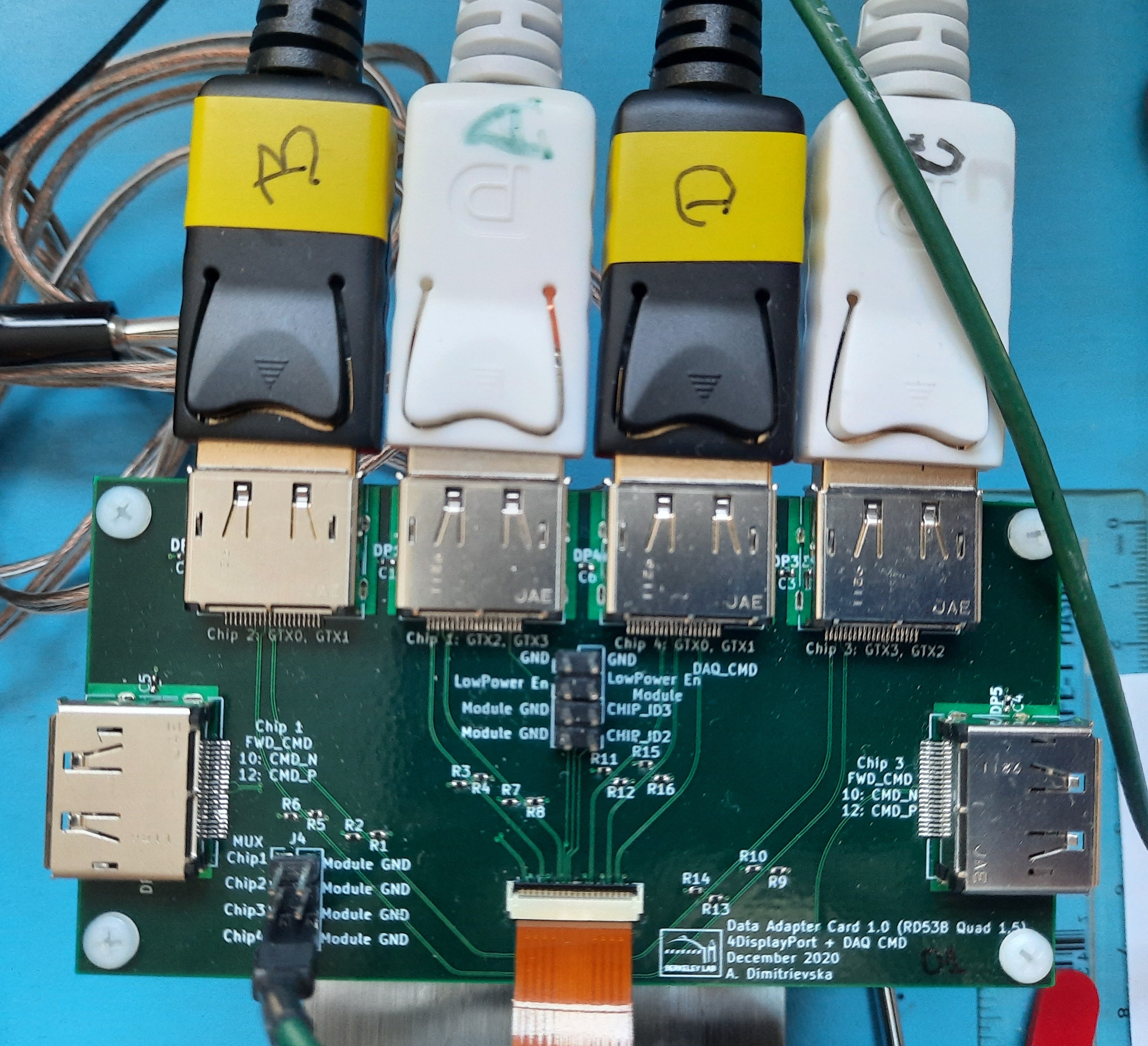
¶ Connectivity Example
¶ Example for 4 DisplayPort Data Adapter Card
This is connectivity example for 4DP data adapter card. The DisplayPort cables are connected to the ports on the Ohio card as shown in the picture and table
| #Chip | Ohio Port |
|---|---|
| Chip 1 | Port A |
| Chip 2 | Port B |
| Chip 3 | Port C |
| Chip 4 | Port D (CMD is provided from here) |
Example of the connectivity file:
{
    "chipType" : "RD53B",
    "chips" : [
        {
            "config" : "configs/rd53b_Quad03_Chip1.json",
            "tx" : 3,
            "rx" : 0,
            "enable" : 0,
            "locked" : 0
        },
        {
            "config" : "configs/rd53b_Quad03_Chip2.json",
            "tx" : 3,
            "rx" : 1,
            "enable" : 0,
            "locked" : 0
        },
        {
            "config" : "configs/rd53b_Quad03_Chip3.json",
            "tx" : 3,
            "rx" : 2,
            "enable" : 1,
            "locked" : 0
        },
        {
            "config" : "configs/rd53b_Quad03_Chip4.json",
            "tx" : 3,
            "rx" : 3,
            "enable" : 0,
            "locked" : 0
        }
    ]
}
Summary table of Chip configs:
| #Chip | ChipID |
DataMergeOutMux0/1/2/3 |
SerEnLane |
|---|---|---|---|
| Chip1 | 12 | 2/3/0/1 | 4 |
| Chip2 | 13 | 3/0/1/2 | 2 |
| Chip3 | 14 | 1/2/3/0 | 8 |
| Chip4 | 15 | 0/1/2/3 | 1 |
¶ Example for 1 DisplayPort Data Adapter Card
This is example for 1 DisplayPort Data adapter card. The DisplayPort is connected to Port A of the Ohio cars. Note that DisplayPort
- pins 1,3 correspond to channel 0
- pins 4,6 to channel 1
- pins 7,9 to channel 2
- pins 10,12 to channel 3
Example of the connectivity file:
{
    "chipType" : "RD53B",
    "chips" : [
        {
            "config" : "configs/rd53b_1DPQuad04_Chip1.json",
            "tx" : 0,
            "rx" : 2,
            "enable" : 1,
            "locked" : 0
        },
        {
            "config" : "configs/rd53b_1DPQuad04_Chip2.json",
            "tx" : 0,
            "rx" : 1,
            "enable" : 0,
            "locked" : 0
        },
        {
            "config" : "configs/rd53b_1DPQuad04_Chip3.json",
            "tx" : 0,
            "rx" : 0,
            "enable" : 0,
            "locked" : 0
        },
        {
            "config" : "configs/rd53b_1DPQuad04_Chip4.json",
            "tx" : 0,
            "rx" : 3,
            "enable" : 0,
            "locked" : 0
        }
    ]
}
Summary table of Chip configs:
| #Chip | ChipID |
DataMergeOutMux0/1/2/3 |
SerEnLane |
|---|---|---|---|
| Chip1 | 12 | 2/3/0/1 | 4 |
| Chip2 | 13 | 0/1/2/3 | 1 |
| Chip3 | 14 | 1/2/3/0 | 8 |
| Chip4 | 15 | 0/1/2/3 | 1 |